Optimizing the Performance of Full adder, NAND by the Use of Parameters of Nano Tube Carbon Field Effect Transistor Technology
Seyedeh Somayeh Hatefinasab
Department of Computer Engineering,Payame Noor University,Sari,Iran.
Received date: September 12,2015; Accepted date: October 30,2015; Published date: October 31,2015
Abstract
Full adder and NAND are the most important parts of digital circuits. Therefore, optimizing the these blocks improves the whole output parameters of digital circuits. In this paper controversial full adder and NAND are designed in CNFET technology and then different parameters of CNFET technology are changed to optimize the speed and power consumption of full adder and NAND. The results of simulation by using HSPICE in .9v are presented. The result of simulation shows the best parameters for better performance of these full adder and NAND in CNFET technology.
Keywords
Controversial full adder; CNFET; Power consumption; NAND; Chirality vector.
Introduction
Delay problem of designed circuits in CMOS technology is very obvious because of intermediate capacitors in integrated circuits. So,the performance of the whole circuits decreases. The reason why capacitor decreases the speed of whole circuit is that the shortage ability of driving current gates driving capacitor charge. This problem of Silicon transistors can be solved by CNFET new technology. CNFET is rolled graphic sheet which is directed in specific vector called chirality vector. This vector is determinate by pair (n1,n2 ) . CNFET is one of the molecular transistor in which many fundamental silicon transistor restrictions are avoided and electron has ballistic or close ballistic transport in channel of CNFET [1,2].
In this paper,two fundamental blocks,full adder and NAND,are simulated in CNFET technology by standard parameters and then by changing these parameters,the best performance can be obtained.
CNFET
In Carbon nanotube field effect transistors,there are nanotubes,which are instead of channel in the structure of CMOS technology. There are two kinds of CNFET transistors: MOSFET-like CNFET and Schottky Barrier CNFET. In source and drain of MOSFET-like,doped carbon nanotubes are used the intrinsic semiconducting carbon nanotubes are implemented in channel region [3,4].
One of the advantages of CNFET is that it threshold voltage can be determinate by using suitable diameter. This relationship between the diameter on CNT and the threshold voltage of the CNFET can be expressed by below equation (1) [5].

The diameter of CNT can be achieved by pair (n1,n2 ) which are parameters of Chirality vector and lattice,that is carbon atom distance. The diameter can be calculated by below equation (2) [5].

In this paper,MOSFET-like CNFET,and to simplify CNFET is used instead of MOSFET-like.
Full adder
One of the important blocks in digital circuits is full adder. Therefore,optimizing full adder can help optimizing the whole performance of digital circuits. Full adder can be implemented by equation (1).


NAND
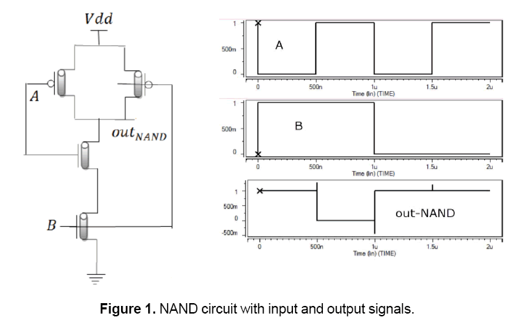
One of basic circuit is 2-input NAND in digital circuit. The pull-down network is complementary. That is to say,when pull-down is ON,the pull-up network is OFF. When pull-up is ON,the pull down circuit is OFF [6]. This circuit in CNFET technology is shown in Figure 1.
Pervious full adder work
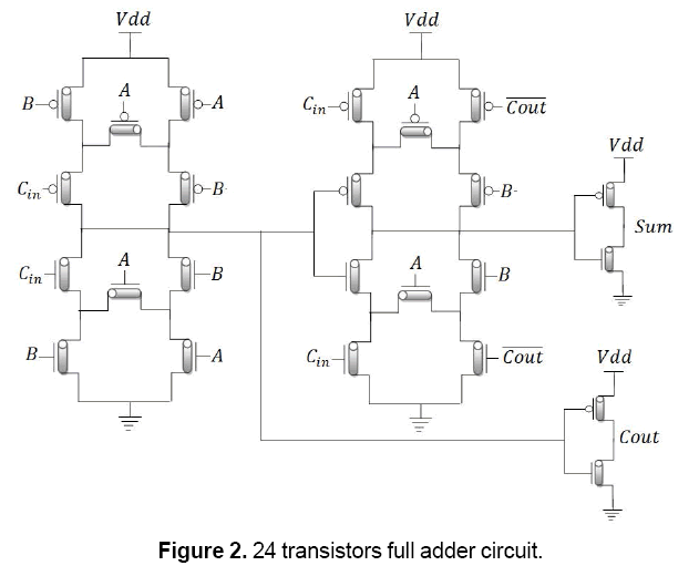
Many full adder blocks are designed in CMOS technology. One of them is 24 transistors [7]. Bridge full adder with 26 transistors is symmetric [8]. 24 transistors have less power consumption in comparison with 26 transistors,because 24 transistors have fewer transistors than 26 transistors. But delay of 24 transistors is more than that of 26 transistors,because of the structure of 24 transistors. Another full adder structure is CPL with 18 transistors [9]. In this circuit,NMOS pass transistors are used. Then another CPL called DPL full adder is designed by extra transistors,with 24 transistors [10]. The problem of CPL is that amplitude of input current cannot be seen in the amplitude of output current. DPL is designed by extra PMOS transistors,so the problem of CPL full adder is not in DPL full adder. Two structures based on XOR/XNOR are HYBRID and NCELL. HYBRID full adder has 26 transistors,which is very high speed and less delay,but the power increases because of extra 4 transistors [11,12]. NCELL has 14 transistors,but the output signal does not have full swing. The last full adder designed is N10T. Because it has minimum number of transistors,it has the best performance and consumption area [13]. The limitation of CMOS transistors can be solved by CNFET. Different full adders are designed in CNFET technology [14-18]. In this paper,full adder is designed in CNFET technology. 24 transistors full adder circuit Figure 2 [19].
Simulation
In this section,24 transistor full adder and NAND are simulated in a compact model of CNFET presented in [2,20]. All simulation is done by Synopsys HSPICE 2008 simulator tool at room temperature.
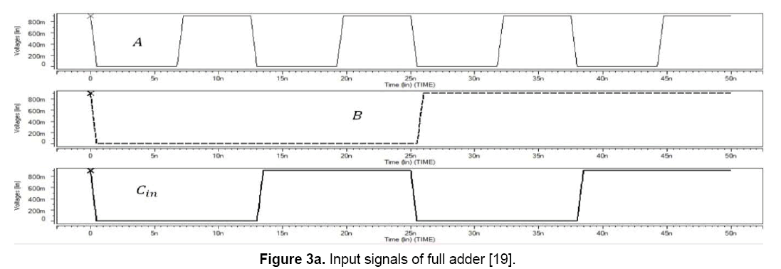
The first circuit simulated is full adder [19]. The input and output signals are shown in Figure 3 . The simulation is done in .9 voltage power supply and 80 MegHz frequencies.
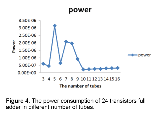
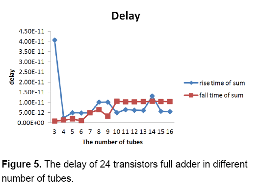
This full adder is simulated by standard parameters of CNFET [19]. In this paper,by changing the parameters of CNFET,the best performance of full adder is achieved. As the most fundamental parameters for full adder are delay,power consumption and powerdelay product (PDP),the performance of full adder is evaluated by these parameters. The first changed parameter is the number of Nano tubes. The standard number of tube is three. The delay,rise time and fall time,power consumption and PDP are calculated by increasing the number of tubes,this number of tubes is the same in N-CNFET and P-CNFET (Figures 4 and 5).
As can be observed in Figure 4 and 5,when the numbers of tubes are in 24 transistor full adder is four,delay and power consumption can be minimized.
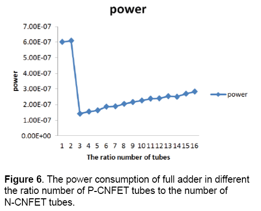
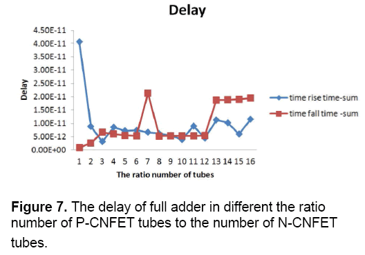
Two Figures 4 and 5 show changes of output signals,when the number of tubes in N-CNFET and P-CNFET are the same. But in the following simulation,the number of tubes in P-CNFET and N-CNFET is not the same. This ratio number is increased to find the best performance of full adder. As Figure 6 reveals that three is the best ratio number of all the number of P-CNFET tubes to the number of all N-CNFET tubes. The power consumption for different ratio number of tubes is shown in Figure 6 .
In Figures 6 and 7 the results of changing the ratio number of P-CNFET tubes to N-CNFET tubes are shown. The standard situation is when the number of tubes in P-CNFET and N-CNFET is three,but the best performance of full adder is when the ratio number is three. That is to say,the number of tubes for P-CNFET is 9 and the number of tubes for N-CNFET is 3.
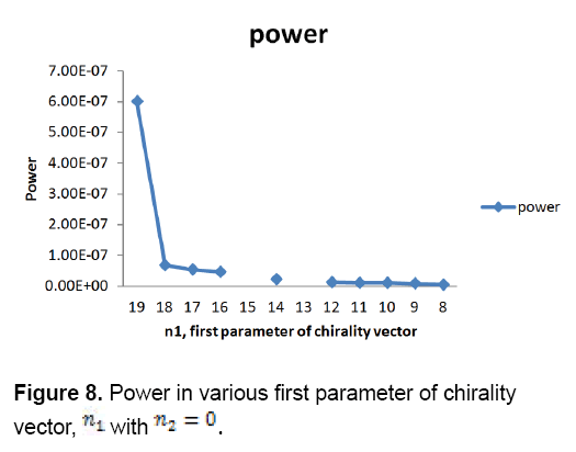
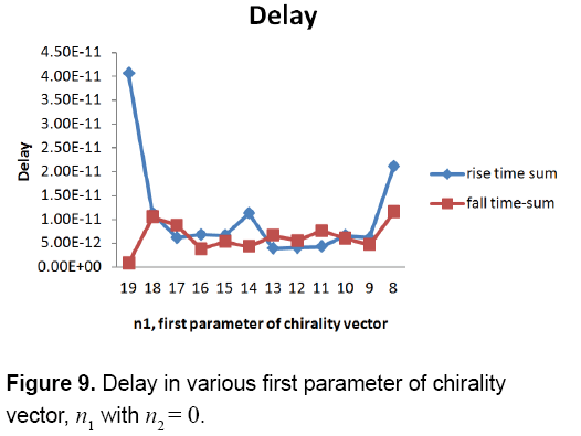
The full adder has different performance in different chirality vectors. Pair (n1,n2). determines chirality vector. In the standard chirality vector is (19,0),the best performance can be achieved by changing n1,from 19 to 8. In all situations,n2 is set zero. Power consumption and delay of these simulations are shown Figures 8 and 9.
In the two chirality vectors,when chirality vectors are (15,0) and (13,0),the power consumptions are very high,at approximately 7.09E watt,so I try to eliminate from the Figure 8 . The power consumption is decreased by decreasing the first chirality vector,n1 but there is not any order in changing the delay. The best performance of full adder is in (12,0) chirality vector. By determining the chirality vector,the diameter of tubes can be calculated.
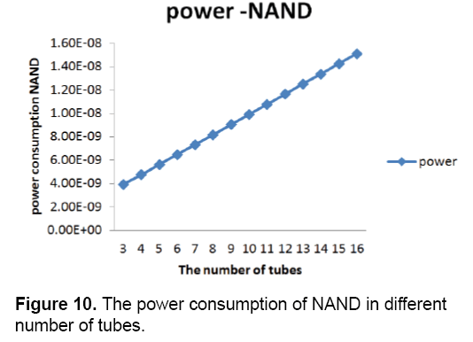
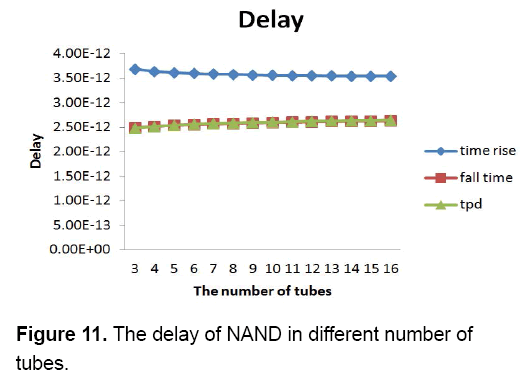
The second circuit simulated is NAND in CNFET technology. The first changed parameter is the number of nano tubes. The delay,rise time and fall time,power consumption are calculated by increasing the number of tubes,this number of tubes is the same in N-CNFET and P-CNFET (Figures 10 and 11).
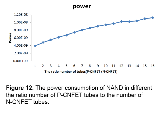
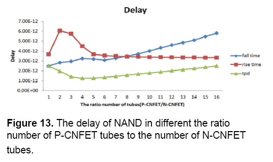
As can be observed,increasing the number of tubes in NAND circuit does not have any positive effects on power consumption and delay,so the best number of tubes in NAND is three. In the following simulation,the number of tubes in P-CNFET and N-CNFET is not the same. The ratio number of two P-CNFET tubes to the number of two N-CNFET tubes is increased to find the best performance of NAND (Figures 12 and 13).
In Figure 12,the power consumption increases by increasing the number of tubes,but the delay line has the minimum,when the ratio is three. That is to say,the number of tubes in P-CNFET is 9 and the number of tubes in N-CNFET is 3.
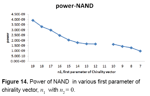
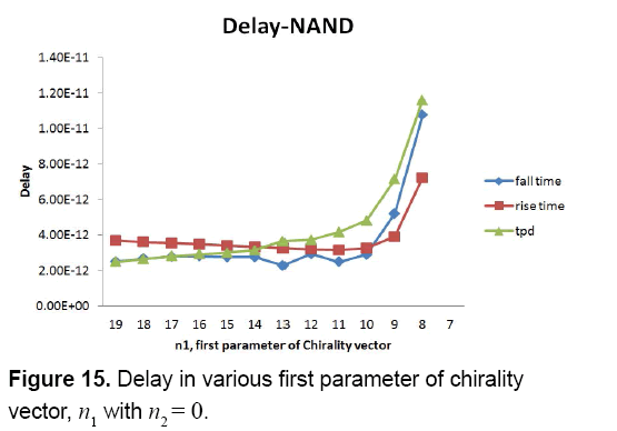
In the following stage,the 2-input NAND gate is simulated by changing the n1 first parameters of pair chirality vector,(n1,n2) (Figures 14 and 15).
As can be observed in Figure 14,the one power is not show,because it is very high,at approximately 1.62E- 02 watt and it shown that the power consumption of NAND decreases by decreasing the first parameter of chirality vector. In Figure 15,the delay of NAND indicated by changing the first parameter of chirality vector,(n1,n2). The delay of (7,0) chirality vector is not shown,because it is very high in comparison with other delays. The best chirality vector for NAND is (12,0),because in this chirality vector,multiplication of power and delay has the minimum value.
Conclusion
In the CNFET technology,the performance of fundamental circuits such as full adder and NAND is better than CMOS technology,because the ballistic behavior of electron in nanotube carbon in channel. Another advantage of the CNFET is by changing the parameters of CNFET,the performance of circuit can be optimized. In the full adder,if the number of tubes for all CNFET in full adder is 4,the best performance can be achieved. By increasing the number of tubes in P-CNFET in comparison with the number of tubes in N-CNFET,the best performance of full adder can be obtained. The best ratio number of tubes is 4. Also,the full adder performance can be improved by changing the chirality vector. In (12,0) chirality vector the better result can be obtained. By doing all this simulation for NAND circuit,the performance of NAND is not affected by the number of tubes,when this number is the same in N-CNFET and P-CNFET. So the standard number of tubes can be the best choice,3. The best performance can be obtained,when the ratio number of P-CNFET tubes to the number of N-CNFET tubes is 4. By changing the chirality vector,the best direction is (12,0) chirality vector in NAND.
References
- A Raychowdhury,K Roy. (2005). Carbon-Nanotube-Based Voltage-Mode Multiple-Valued LogicDesign.IEEE Trans. Nanotechol. 4:168-179.
- J Deng,H-SP Wong. (2007). A Compact SPICE Model for Carbon- Nanotube Field-Effect Transistors Including Nonidealities and Its Application: Part II: Full Device Model and Circuit Performance Benchmarking. IEEE Trans. Electron Devices. 54: 3195-3205.
- Abdolahzadegan SH,Keshavarzian P,Navi K. MVL. (2010). Current Mode Circuit Design Through CarbonNanotube Technology. European Journal of Scientific Research. 42:152-163.
- Javey A,Guo J,Wang Q,Lundstrom M,Dai H. (2003). Ballistic carbon nanotube field-effect transistor.Nature.424:654-657.
- Y Bok Kim,Y B Kim,F Lombardi. (2009). In Proc. IEEE International Midwest Symposium on Circuits and Systems 1130.
- Prashant Gupta,Aminul Islam. (2014). Robustness Study and CNFET Realization of Optimal Logic Circuit for Ultralow Power Applications.International Conference on Signal Processing and Integrated Networks.
- KeivanNavi,OmidKavehei,MahnousRuholamini,et al. (2008). AmirSahafi,ShimaMehrabi and NooshinDadkhahi,“Low-Power and High-Performance 1-Bit CMOS Full Adder Cell.Journal of Computers. 3.
- O Kavehei,MRahimiAzghadi,K Navi,AP Mirbaha. (2008). Design of Robust and High-Performance 1-bit CMOS Full Adder for Nanometer Design. IEEE computerSociety AnnualSymposium on VLSI,ISVLSI’08.
- DimitriosSourdis,Christian Piguet,Costas Goutis. (2004). Designing CMOS Circuits for Low Power.European Low-Power Initiative for Electronic System Design Kluwer Academic Publishers.
- CH Chang,J Gu,M Zhang. (2005). A review of 0.18µm full adder performances for tree structured arithmetic circuits.IEEE Transactions on Very Large Scale Integration (VLSI) Systems. 13: 686-695.
- ArashShoarinejad Sue Ann Ung,WaelBadawy. (2003). Low Power Single Bit Full Adder Cells,Can. Jl. of Electrical and Computer Engineering. 28: 3-9.
- SGosel,ShilpaGollamudi,Ashok Kumar,MagdyBayoumi. (2004). On the Design of Low-Energy Hybrid CMOS 1-Bit Full Adder Cells”,47th IEEE International Midwest Symp. on Circuits and Systems. 2: 209- 211.
- FartashVasefi,Z Abid. (2005). Low Power N-bit Adders and Multiplier Using Lowest Number of Transistors 1-bit Adders”,IEEE conference proceeding of CCECE/CCGEI,Saskatoon. 1731-1734.
- K Navi,AMomeni,F Sharifi,PKeshavarzian. (2009).Two novel ultra-high speed carbon nanotube Full-Adder cells. IEICE Electronics Express. 6: 1395-1401.
- K Navi,R Sharifi Rad,MH Moaiyeri,AMomeni. (2010). A Low-Voltage and Energy Efficient Full Adder Cell Based on Carbon Nanotube Technology. Nano Micro Letters. 2: 114-120.
- K Navi,M Rashtian,A khatir,P Keshavarzian,O Hashemipour. (2010) High Speed Capacitor- Inverter Based Carbon Nanotube Full Adder. NanoscaleRessLett. 5: 859-862.
- AshkanKhatir,Shaghayegh Abdolahzadegan,Iman Mahmoudi. (2011). High speed multiple valued logic full adder using carbon nano tube field effect transistor.International Journal of VLSI design & Communication Systems (VLSICS). 2.
- Ali Ghorbani,Mehdi Sarkhosh ,ElnazFayyazi ,Neda Mahmoudi ,PeimanKeshavarzian. (2012). A novel full adder cell based on carbon nanotube field effect transistors.International Journal of VLSI design & Communication Systems (VLSICS).3.
- عمج مامت کی یحارط " ,نامیپ نایزرواشک ، ینابرق یلعینادیم رثا ياهروتسیزنارت زا هدافتسا اب دیدج هدننکیاه هدیا سنارفنک نیلوا "ینبرک ياه هلول ونانرب ینتبم. قرب یسدنهم رد ون1391,
- Jie Deng,HS Philip Wong. (2007). A Compact SPICE Model for Carbon-Nanotube Field-Effect Transistors Including Non idealities and Its Application—Part I: Model of the Intrinsic Channel Region. IEEE. 54.

Open Access Journals
- Aquaculture & Veterinary Science
- Chemistry & Chemical Sciences
- Clinical Sciences
- Engineering
- General Science
- Genetics & Molecular Biology
- Health Care & Nursing
- Immunology & Microbiology
- Materials Science
- Mathematics & Physics
- Medical Sciences
- Neurology & Psychiatry
- Oncology & Cancer Science
- Pharmaceutical Sciences
