Design a Low Power CNTFET-Based Full Adder Using Majority Not Function
Seyedehsomayeh Hatefinasab
Department of Electrical and Computer Engineering, Payame Noor University, Sari, Iran.
- Corresponding Author:
- Seyedehsomayeh Hatefinasab
Department of Electrical and Computer Engineering
Payame Noor University, Sari, Iran
Tel: 989370657242
E-mail: hatefinasab@gmail.com
Received date: December 12, 2015; Accepted date: January 10, 2016; Published date: January 16, 2016
Citation: Hatefinasab S, Design a Low Power CNTFET-Based Full Adder Using Majority Not Function. Electronic J Biol, 12:1
Abstract
In this paper, a Majority Not Function-based full adder using (Carbon Nano Tube Field Effect Transistor) CNTFET technology is presented. The better performance of a full adder using CNTFET technology in comparison with full adders using CMOS technology can be shown in the simulation results. Power, delay and power delay product (PDP) are measured to prove this optimized performance. The full adders are at 90nm CMOS process technology and CNFET technology at a three-volt supply source.
Keywords
Dynamic full-adder; CNTFET; CMOS.
Introduction
Scaling down the feature size towards nano scale causes CMOS technology to become less affective. Some problems can be emerged, such as decreased gate control, short channel effects and high leakage power consumption [1]. To solve these problems of conventional CMOS technology, Quantum Dot Cellular Automata, Single Electron Transistor and Carbon Nano Tube Field Transistor are introduced as nanotechnologies [2,3]. However, Carbon Nano Tube Field Transistor could be a more superior alternative than others, because CMOSs and CNTFETs are similar to each other except the channel region which is the intrinsic semiconducting Carbon Nano Tube in CNTFET technology [4]. In this Nano Tubes, transport is near ballistic [5].
The better properties of CNTFETs like low power and high performance may make them interesting to be used in the integrated circuits. One of the fundamental blocks of integrated circuits is full adder [6]. Many attendances have been done to optimize the full adders [7-11]. In this paper, CNTFET technology is applied to improve the performance of full adder by using HSPICE at a three-volt supply source.
CNFETs
Carbon Nano Tubes (CNTs) are hollow cylindrical sheets of graphite [12]. The direction of Nano Tubes is determinate by chirality vector that is determinate by a pair of integers.This chirality vector is shown in Figure 1. The Nano Tube diameter can be calculated by this pair chirality vector with Equation (1) [13].
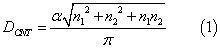
Where, α is lattice constant which means carbonto- carbon bond distance, at approximately 2.49A (Figure 1) [14].

Figure 1: A) Single nano tube. B) Graphite sheet and chirality vector [14].
Since the diameter of CNTs is proportional to band gap, the threshold voltage can be controlled by adjusting the diameter of intrinsic CNTs, which is given by Equation (2) [13].
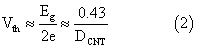
In this paper, the standard parameters of CNFETs are applied such as a pair of integers (n1, n2) = (19,0) and this chirality vector can be used for define the diameter of CNTs which is calculated 1.487 nm by using Equation (2), the threshold voltage is 0.293 V. The full adder is optimized based on MOSFETlike CNFET; therefore the term of CNFET instead of MOSFET-like CNFET is applied. The schematic of CNFET is shown in Figure 2 [15].

Figure 2: Diagram of a carbon nanotube transistor [15].
Previous works
Several CMOS logic styles have been applied to implement a full adder block [16-19]. Some of these logic styles are selected for comparison in this paper, which is shown in Figure 3 [20]. All these circuits are full adders which have different intermediate nodes, number of transistors and critical paths. These different features are made for various applications in which needs one parameter of an output full adder, such as area, delay and power consumption. Some of full adders apply one or more than one style in their structures. In the following passage, some points about various full adders are presented.

Figure 3a: The conventional CMOS full adder (CCMOS) [21].
The complementary CMOS full adder (C-CMOS) with 28 transistors is shown in Figure 3(a) [21]. This full adder has pull-up and pull-down transistors. All inputs are connected to the gates of transistors; therefore, the input capacitances of static CMOSs are considerable. Two buffers are used in the output nodes to drive the weakest drive.

Figure 3b: The 10- transistor full adder (10T) [20].
Another style is used for full adders is 10-transistors full adder in Figure 3(b) [20]. This full adder designed based on hybrid logic style [22]. It has the small transistor account, but it does not have full swing. One of disadvantages of this full adder is the lack of driving capabilities in fan-out situation. The cascaded of 10-transistors full adders cannot drive very well. The A⊕ B is generated in this full adder and then this signal is used to generate the output signals.
The third full adder is Hybrid. Hybrid has 26 transistors, which works based on XOR/XNOR gates and inverters and complementary CMOS style [23]. The output signals of this full adder are full swing. This Hybrid full adder is shown in Figure 3(c).

Figure 3c: Hybrid full adder.
The full adder using Majority Not Function with linear input capacitors and CMOS inverters is shown in Figure 3(d) [20]. There are many reasons that this full adder has low power consumption. First, a reduction in the number of transistors can help low switched capacitance. Second, having just two transistors from power supply to the ground is resulted from using robust CMOS inverters. Lastly, short circuit current is eliminated at low voltage 

Figure 3d: Full adder using majority not function [20].
This full adder using Majority Not Function is able to work at low power supply, but consumes high area and has capacitance effects on three input signals because there are three input capacitors connected to input signal nodes. To illustration a Majority function based full adder which has been designed, each input is connected to two capacitors which reduce the reliability of a full adder because of charge sharing in these two capacitors [24]. In the previous design of Majority Not Function [24], there is one vote for each capacitor in each input full adder. Therefore, two capacitors in input signals are derived by  . These two capacitors can be replaced by one capacitor which has two votes. When one capacitor has two votes, which means it has 2 times higher capacitance value.
This full adder which is shown in Figure 3(d) consumes less area in comparison with other majority based full adders because of less capacitors applied. Another advantage is that each input capacitor is connected to one input signal, which increases the reliability of full adder. Also, this full adder can drive highly efficiency.
Proposed full adder
This majority-based full adder was simulated using CNTFET technology. The output parameters of this full adder are compared to this full adder using CMOS technology. Each capacitor is only one chance in Majority Not Function-based full adder to drive 0°C which derives two capacitors which can be replaced by a capacitor having two chances (Figure 4).

Figure 4: Majority not function full adder using CNTFET technology.
Simulation
The results of simulation by using HSPICE a threevolt supply source, 0.45 V, 0.5 V and 0.55 V are presented. The results of simulations show the best parameters for Majority Not Function full adder using CNTFET technology. The threshold of NMOS is 0.22 V and the threshold voltages of PMOS are 0.31 V at 90 nm CMOS technology. The input and output signals of Majority Not Function full adder using CNTFET technology at 0.5 V supply voltage are shown in Figure 5.

Figure 5: Input and output signals of majority not function full adder using CNTFET technology.
The simulation results are shown in Table 1. Four full adders, C-CMOS, 10 Transistors, Hybrid and Majority Not Function based full adder using 90 nm CMOS and Majority Not Function based full adder using CNTFET technology at 0.45 V, 0.5 V and 0.55 V. The new Majority Not Function full adder using CNTFET technology consumes 90.5%, 82.5%, 98.5% and 72% less power consumption than C-CMOS, 10Transistors, Hybrid and Majority Not Function full adder using CMOS at 0.5 V. The delay of full adder is also improved slightly by using CNTFET technology.
| vdd | 0.45v | 0.5v | 0.55v |
| Delay (nsec) | |||
| Proposed Majority not function full adder using CNTFET | 1.3542 | 1.1302 | 0.8108 |
| Majority not function full adder using cmos | 2.00 | 1.36 | 1.05 |
| 28Transistors | 2.04 | 1.14 | .986 |
| 10Transistors | 1.52 | 1.221 | .935 |
| Hybrid | 2.56 | 1.54 | .919 |
| Power(nw) | |||
| Proposed Majority not function full adder using CNTFET | 1.8650 | 2.5110 | 3.5876 |
| Majority- not function full adder using CMOS | 6.84 | 9.08 | 12.3 |
| 28 Transistors | 20.8 | 26.6 | 33.1 |
| 10 Transistors | 11.5 | 14.4 | 17.8 |
| Hybrid | 86.4 | 173 | 337 |
| PDP(J*10-18) | |||
| Proposed Majority not function full adder using CNTFET | 2.52557 | 2.8395 | 2.9727 |
| Majority not function full adder using CMOS | 41 | 12.3 | 14 |
| 28 Transistors | 42.4 | 30.4 | 22.7 |
| 10 Transistors | 15.1 | 11.8 | 95 |
| Hybrid | 221 | 266 | 310 |
Table 1: The result simulations of pervious full adders at 90 nm CMOS and majority not function full adder using CNTFET technology.
The driving capability of full adder in different load capacitors is one of the important features, which can be tested by load capacitors from 2 ff to 10 ff connected to two output nodes. Then, the delay of various full adders is measured at 0.5 voltage power supply and 20 MegHz input frequency. These comparisons are shown in Figure 6.

Figure 6: Various delays of full adders in different load capacitors.
The Figure 6 shows that the lowest delay is for Majority Not Function full adder based on CNTFET technology. The immunity of accurate performance of full adders at different temperatures should be considered. Therefore, all full adder based on CMOS and Majority Not Function full adder based on CNTFET technology are simulated at various temperature from 0°C to 80°C. This simulation is shown in Figure 7.

Figure 7: PDP of different full adders at various temperatures.
As can be observed, the only Majority Not Function full adder based on CNTFET technology can tolerate the higher temperature than 25°C which is room temperature. The CMOS based full adders cannot operate at 30°C, while Majority Not Function full adder based on CNFET technology can operate until 80°C. The littlest delay is related to Majority Not Function full adder based on CNTFET technology from 0°C to 80°C.
Conclusion
A new Majority Not Function full adder using CNTFET technology is presented at a three-volt supply source, 0.45 V, 0.5 V and 0.55 V. This new full adder using CNTFET works in low voltage with high performance. The better performance of new design full adder is proved in comparison with other pervious full adders in different load capacitors and temperatures. The evaluations of full adder performance are done based on Power consumption, delay and PDP parameters. This Majority Not Function full adder has not only less short circuit current because of dynamic structure, but also CNTFET transistors which make better performance.
References
- K Navi, A Momeni, F Sharifi, P Keshavarzian. (2009). Two novel ultra-high speed carbon nanotube Full-Adder cells. IEICE Electronics Express. 6: 1395-1401.
- Tawfik SA, Liu Z, Kursun V. (2007). Independent-gate and tied-gate FinFET SRAM circuits: design guidelines for reduced area and enhanced stability. In: Proceedings of the International Conference on Microelectronics (ICM). 171-174.
- G Cho, Y B Kim, F Lomoverlinedi, M Choi. (2009). Performance evaluation of CNFETbased logic gates, Proc. Instrumentation and Measurement Technology Conference (IMTC), Singapore. 909-912.
- Abdolahzadegan SH, Keshavarzian P, Navi K. (2010). MVL Current Mode Circuit Design through CarbonNanotube Technology. European Journal of Scientific Research. 1:152-163.
- Raychowdhury A, Roy K. (2005). Carbon-Nanotube-Based Voltage-Mode Multiple-Valued Logic Design. IEEE Trans. Nanotechnology. 2:168-179.
- R F Mirzaee, M H Moaiyeri. (2011). A new robust and high-performance hybrid full addercell.J. Circ. Syst. Comput.20: 641-655.
- S Hatefinasab. (2015). Optimizing the Performance of Full adder, NAND by the Use of Parameters of Nano Tube Carbon Field Effect Transistor Technology. Electronic Journal of Biology. 11: 104-109.
- J P Uyemura. (2002). Introduction to VLSI Circuits and Systems, John Wiley& Sons, New York, NY, USA.
- S M Kang, Y Leblebici. (2003). CMOS Digital Integrated Circuits: Analysis and Design, Tata McGraw-Hill, New York, NY, USA.
- N Weste, D Harris. (2005). CMOS VLSI Design, Pearson Wesley.
- N Weste, K Eshraghian. (1993). Principles of CMOS VLSI Design: A System Perspective, Addison-Wesley, Reading, Mass, USA.
- Lin J, Hwang Y A. (2007). Novel High-Speed and Energy Efficient 10-Transistor Full Adder Design. IEEE Transactions on Circuits and Systems.54: 1050-1059.
- Javey A, Farmer D, Guo J, et al. (2005). High-performance n-type carbon nanotube field-effect transistors with chemically doped contacts. Nano Lett.5: 345.
- Fahad Ali Usmani, Mohammad Hasan. (2010). Carbon nanotube field effect transistors for high performance analog applications: An optimum design approach.Microelectronics Journal. 41: 395-402.
- Peiman Keshavarzian. (2013). Novel and general carbon nanotube FET-based circuit designs to implement all of the 39 ternary functions without mathematical operations.Microelectronics Journal. 44: 794-801.
- D. Radhakrishnan. (2011). Low-voltage low-power CMOS full adder Proc. IEE Circuits, Devices and Systems.148: 19-24.
- A Shams, M Bayoumi. (1999). Performance evaluation of 1-bit CMOS adder cells in Proc. IEEE Int. Symp. Circuit and Systems. 27-30.
- S. Goel, A Kumar, M A Bayoumi. (2006). Design of robust, energy efficient full adders for deep-sub micrometer design using hybrid-CMOS logic style." Very Large Scale Integration (VLSI) Systems.IEEE Transactions on 14.12: 1309-1321.
- M Zhang, J Gu, C H Chang. (2013). A novel hybrid pass logic with static CMOS output drive full-adder cell." Circuits and Systems,2003. ISCAS'03. Proceedings of the 2003 International Symposiumon. Vol. 5. IEEE.
- Vahid Foroutan, Keivan Navi. (2015). Low Power Dynamic CMOS Full-Adder Cell. International Journal of Computer Science and Information Technologies. 6: 3198-3201.
- R Zimmermann, W Fichtner. (1997). Low-Power Logic Styles: CMOSversus Pass-Transistor Logic.IEEE J. of Solid-State Circuits. 32: 1079-1089.
- H T Bui, Y Wang, Y Jiang. (2002). Design and analysis of lowpower 10-transistor full adders using novel XOR-XNOR gates.IEEE Trans. Circuits Syst. II, Analog Digit. Signal Process. 49: 25-30.
- Chang C H, Gu J, Zhang M. (2005). A review of 0.18-μm full adder performances for treestructured arithmetic circuits.IEEE Transactions on Very Large Scale Integration Systems. 13: 686-695.
- K Navi, M Maeen, V Foroutan, S Timarchi, O Kavehei. (2009). A novel low power full-adder cell for low voltage.Integration. the VLSI journal.


Open Access Journals
- Aquaculture & Veterinary Science
- Chemistry & Chemical Sciences
- Clinical Sciences
- Engineering
- General Science
- Genetics & Molecular Biology
- Health Care & Nursing
- Immunology & Microbiology
- Materials Science
- Mathematics & Physics
- Medical Sciences
- Neurology & Psychiatry
- Oncology & Cancer Science
- Pharmaceutical Sciences